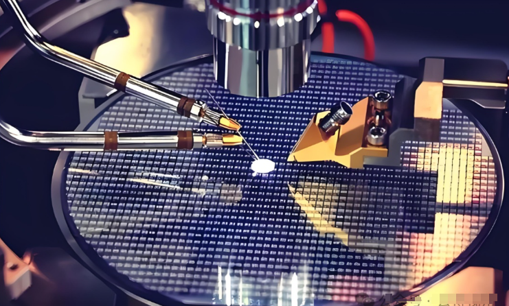
Out on the fab floor, a lab-on-a-chip run goes sideways when the drying step drifts. You spot edge bead, scumming in the channels, and yield slipping on 300 mm wafers. The heater has to follow the recipe, not the room temperature.
What matters, technically
We built the lab-on-a-chip drying heater around short-wave infrared emitters in a quartz-ceramic module. Fast response, low thermal mass—exactly what you need. Wafer-level uniformity stays at ±0.1°C across the bake zone, so your soft bake and hard bake profiles for photoresist don’t wander outside spec. It’s engineered for Class 1–100 cleanrooms: sealed housings, HEPA-grade materials, and zero particle generation under continuous operation. Repeatability is the point—setpoint to measured temperature tracks in a tight band, cycle after cycle.
Why it fits the work we do
This heater hits the pain points in wafer fabrication and packaging: consistent drying after cleaning, stable bakes for lithography, and predictable thermal budgets across lots. Tight uniformity cuts photoresist defects and edge effects, which shortens qualification cycles and reduces scrap. Energy use drops because the emitters ramp quickly and hold steady without overshoot. Reliability has been proven on 24/7 schedules, with zero unplanned downtime in line trials.
What you need to know up front
Installation means matching the tool interface and confirming voltage and connector specs for your platform. The footprint fits standard process stations, but you still need clearance around the emitter zone for airflow and particle control. Plan for periodic calibration checks to keep that ±0.1°C uniformity. This isn’t set-and-forget—it’s part of the process discipline.